Unit 1 · 3 teaching hours · 16 min read
Introduction: Digital Signals, Logic Levels and the Clock
What the syllabus asks for 5
- Analog and digital signals
- Logic levels and logic polarity
- Pulses and the clock waveform
- Digital logic operations and integrated circuits
- Advantages and applications of digital systems
Every program you will ever write finally runs on circuits that know only two conditions: a voltage that is high and a voltage that is low.
Digital logic is the study of how such two-valued signals are combined to do arithmetic, remember values and keep time. It is the bridge from the transistor to the CPU.
- Analog vs digital signals, and why computers chose digital.
- Logic levels, noise margin, positive and negative logic.
- Pulse and clock waveform terms: period, frequency, duty cycle, rise/fall time.
- Integrated circuits: SSI, MSI, LSI, VLSI and the logic families TTL and CMOS.
1.1 Analog and digital signals
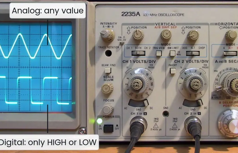
An analog signal varies continuously (a microphone voltage, temperature). A digital signal takes only a few discrete values, almost always two, written 0 and 1.
| Analog | Digital | |
|---|---|---|
| Values | continuous | discrete (0 and 1) |
| Noise | accumulates and cannot be removed | a small disturbance is ignored; signal can be regenerated |
| Storage | degrades on copying | exact copies, error detection and correction possible |
| Circuits | amplifiers, filters | gates, flip-flops, easy to integrate in huge numbers |
| Accuracy | limited by component tolerance | set by the number of bits |
Digital wins because a threshold decision removes noise: a 0.2 V ripple on a 5 V line changes nothing, but the same ripple on an analog audio signal is heard.
Real-world quantities are converted with an ADC (analog-to-digital converter) on input and a DAC on output.
A signal is sampled (measured at regular instants) and quantised (rounded to one of 2ⁿ levels); an n-bit ADC over a range V gives a step of V / 2ⁿ. For example 8 bits across 0–5 V gives 5 / 256 ≈ 19.5 mV.

1.2 Logic levels and logic polarity
A digital circuit does not need an exact voltage, only that a signal falls inside the high band or the low band. For standard 5 V TTL:
| Quantity | Meaning | TTL value |
|---|---|---|
| V_IL(max) | highest input still read as 0 | 0.8 V |
| V_IH(min) | lowest input read as 1 | 2.0 V |
| V_OL(max) | worst-case output for 0 | 0.4 V |
| V_OH(min) | worst-case output for 1 | 2.4 V |
The voltage between 0.8 V and 2.0 V is the forbidden (undefined) region. The noise margin is how much noise a signal can carry and still be read correctly: NM_H = V_OH(min) − V_IH(min) = 2.4 − 2.0 = 0.4 V; NM_L = V_IL(max) − V_OL(max) = 0.8 − 0.4 = 0.4 V.
Positive logic: high = 1, low = 0. Negative logic: high = 0, low = 1. Under positive logic a gate that behaves as AND behaves as OR in negative logic; this is the duality used in De Morgan's theorem. Unless stated, assume positive logic.
Logic families. TTL (transistor-transistor logic, 74xx series, 5 V) was the classic family.
CMOS (74HCxx, 4000 series) uses almost no power when idle, works over a wide supply range, and dominates today; every microprocessor and memory is CMOS.
Comparison: CMOS has far lower static power and, at low supply voltage, can be made as fast as TTL; classic bipolar TTL draws milliwatts per gate even when idle. Fan-out is how many gate inputs one output can drive.

1.3 Pulses and the clock waveform
An ideal digital waveform is a square wave; a real one has a rise time t_r and fall time t_f, usually measured between 10 % and 90 % of the amplitude, and a propagation delay t_pd: the time from an input change to the output change.
For a periodic clock:
- Period T: the time of one complete cycle.
- Frequency f = 1 / T (hertz).
- Duty cycle = t_high / T × 100 %.
A 50 MHz clock has T = 1 / (50 × 10⁶) = 20 ns. A clock with a 6 ns high time in a 20 ns period has a 30 % duty cycle.
Edge terms matter for sequential circuits: the positive (rising) edge is the 0 → 1 transition, the negative (falling) edge is 1 → 0. A flip-flop triggered by an edge samples its input at that instant only.
Two timing requirements follow: the data must be stable for a setup time before the edge and a hold time after it.
If a path through gates takes longer than the clock period minus setup, the circuit fails; this is why there is a maximum clock frequency.

1.4 Digital logic operations and integrated circuits
Three basic operations underlie everything: AND (output 1 only if all inputs are 1), OR (output 1 if any input is 1), NOT (inversion). Unit 3 treats them fully. All digital computers, from a calculator to a data centre, are built from millions of these.
Integrated circuit (IC) scale of integration
| Scale | Gates per chip | Example |
|---|---|---|
| SSI (small) | < 12 | 7400 quad NAND |
| MSI (medium) | 12 – 99 | 74138 decoder, 7483 4-bit adder, counters |
| LSI (large) | 100 – 9,999 | small memory, early microprocessors |
| VLSI (very large) | 10,000 – 1,000,000 | 8086 (about 29,000 transistors) onwards |
| ULSI | > 1,000,000 | modern CPUs with billions of transistors |
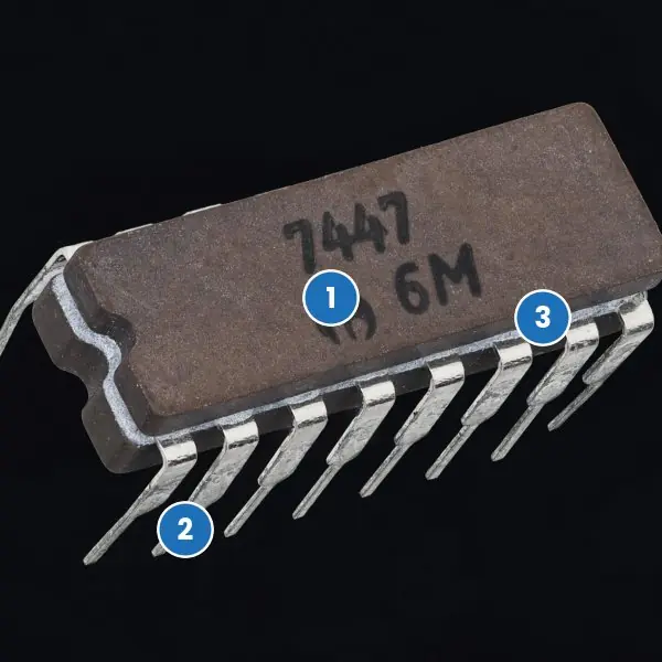
(Boundaries differ slightly between books; learn the order and the examples.) ICs come in DIP (dual in-line package) form for breadboards or surface-mount for production.
Chip pins are numbered anticlockwise from the notch; a 14-pin 74xx chip has V_CC on pin 14 and ground on pin 7.
Digital computer. A digital computer is a system of gates and flip-flops organised as a CPU (ALU + control unit + registers), memory and I/O, all synchronised by a clock.
Understanding how a gate becomes an adder, and a flip-flop becomes a register, is the purpose of this subject.

1.5 Advantages and applications of digital systems
Digital systems are not used only because they are modern. They are used because a two-level signal is easy to protect, copy, store and process. Eight advantages explain why a phone call, a bank transfer and a photograph all travel as bits today.
- Noise immunity. A digital receiver only asks "is this signal above or below the threshold?" A small ripple of 0.2 V on a 5 V line does not change the answer. This is why a Fonepay QR payment gives the same amount at the shop and in the bank, even over a poor mobile network.
- Exact copying and storage. A stored number can be copied millions of times with no loss, while a tape copy of an analog song becomes noisier each time. A scanned citizenship certificate in the Nagarik App is bit-for-bit identical to the original file. Memory chips store these bits as charge or magnetic states.
- Error detection and correction. Extra check bits (parity, CRC, Hamming code) can be added to the data. The receiver detects a flipped bit and, with the right code, repairs it. Banking switches such as NCHL's ConnectIPS depend on such checks to avoid wrong credit.
- Easy integration on silicon. All logic is built from a few simple gates, and the same gate layout can be repeated millions of times. This is why a modern CPU with billions of transistors costs only a few thousand rupees. Analog circuits need large, precise components and do not shrink so well.
- Programmability. The same hardware can do a new job by changing the stored program or the data. A single microcontroller can run an ATM screen today and a ticket machine tomorrow. Analog circuits need new components for each new function.
- Accuracy that is chosen, not hoped for. The accuracy of a digital result depends on the number of bits, so adding bits adds accuracy. A 12-bit ADC separates 4096 levels, while a 16-bit ADC separates 65,536. The Department of Hydrology and Meteorology can log river levels at the resolution it needs.
- One format for every kind of information. Text, sound, pictures and video all become bits, so one network carries all of them. Nepal Telecom sends a voice call, a message and a video over the same digital core. This sharing lowers the cost of equipment and cables.
- Easy processing, encryption and compression. Once data is digital, a program can compress it, encrypt it or search it in seconds. The e-Passport, the Tribhuvan University EMIS and online result systems store records in such compact, protected form.
Limitations. Digital systems need sampling and quantisation, so some information is lost (quantisation error).
They need more bandwidth than a simple analog signal, a clock, and A/D and D/A converters at the boundary with the real world. A power failure can erase volatile memory.
Formula and fact sheet
- Step of an n-bit ADC = V_range / 2ⁿ.
- NM_H = V_OH(min) − V_IH(min); NM_L = V_IL(max) − V_OL(max).
- f = 1 / T; duty cycle = t_high / T.
- Positive logic: H = 1. Negative logic: H = 0. AND ↔ OR under logic inversion.
- TTL thresholds: 0.8 / 2.0 V in, 0.4 / 2.4 V out.
Chapter summary
- Digital signals resist noise because they are decided by thresholds.
- Logic levels have guaranteed bands and a forbidden zone; noise margin measures the safety.
- Clocks are described by period, frequency, duty cycle and edges; setup and hold times limit speed.
- ICs range from SSI gates to ULSI processors; CMOS is the dominant family.
Practice
- List four advantages of digital over analog representation.
- A TTL gate has V_OH(min) = 2.4 V, V_IH(min) = 2.0 V, V_OL(max) = 0.4 V, V_IL(max) = 0.8 V. Compute both noise margins.
- A 12-bit ADC has a 0–3.3 V input range. What is its resolution in millivolts?
- A clock runs at 25 MHz with a duty cycle of 40 %. Find the period and the high time.
- Distinguish positive and negative logic. What does an AND gate become under negative logic?
- What do setup and hold time mean, and what happens if they are violated?
- Name the scale of integration ofaa 7400 chip,ba 4-bit counter chip,ca modern CPU.
Answers and worked solutions
1. Noise immunity; exact storage and copying; error detection and correction; easy large-scale integration; programmability.
2. NM_H = 2.4 − 2.0 = 0.4 V; NM_L = 0.8 − 0.4 = 0.4 V.
3. 3.3 / 4096 = 0.000806 V ≈ 0.81 mV.
4. T = 1 / 25 MHz = 40 ns; high time = 0.4 × 40 = 16 ns.
5. Positive logic takes the high voltage as 1; negative logic takes it as 0. A gate that is AND in positive logic is OR in negative logic.
6. Setup: the data must be stable for a minimum time before the active clock edge; hold: it must stay stable for a minimum time after. Violating them can leave the flip-flop in an undefined (metastable) state or capture the wrong value.
7.(a) SSI,(b) MSI,(c) ULSI (VLSI in older classification).
Model answers: medium (5 marks) and long (10 marks) questions
Q (5 marks). Differentiate analog and digital signals and state any four advantages of digital systems.
An analog signal varies continuously and can take any value in a range, such as the voltage from a microphone or a thermometer.
A digital signal takes only a few fixed levels, usually two (HIGH and LOW, written 1 and 0), and changes between them in steps (see Plate 1.1 and Figure 1.1).
To handle an analog quantity digitally, an ADC samples it at regular instants and quantises each sample to the nearest of 2ⁿ levels; an n-bit ADC over V volts has a step of V / 2ⁿ.
For example, a 10-bit ADC over 0–5 V has a step of 5 / 1024 ≈ 4.9 mV.
| Point | Analog | Digital |
|---|---|---|
| Values | continuous | discrete (0 and 1) |
| Noise | accumulates, cannot be removed | removed by thresholding |
| Copying | quality loss each copy | exact copy |
| Circuits | amplifiers, filters | gates, flip-flops |
| Accuracy | limited by component tolerance | set by the number of bits |
Four advantages: (1) noise immunity, because a 0.2 V ripple does not change a decision; (2) exact storage and copying; (3) error detection and correction using parity or CRC; (4) easy integration into chips and programmability.
A Fonepay QR payment shows all four: the amount is the same at the shop and in the bank.
Q (5 marks). Define noise margin. For a TTL gate with V_OH(min) = 2.4 V, V_IH(min) = 2.0 V, V_OL(max) = 0.4 V and V_IL(max) = 0.8 V, find both noise margins and explain their meaning.
A gate does not output an exact voltage. The manufacturer guarantees only that a HIGH output is at least V_OH(min) and a LOW output is at most V_OL(max).
The next gate, in turn, promises to read any input of at least V_IH(min) as HIGH and at most V_IL(max) as LOW.
The noise margin is the extra unwanted voltage that a signal can pick up on the wire between the two gates and still be read correctly (Figure 1.2).
- High-state noise margin: NM_H = V_OH(min) − V_IH(min) = 2.4 − 2.0 = 0.4 V.
- Low-state noise margin: NM_L = V_IL(max) − V_OL(max) = 0.8 − 0.4 = 0.4 V.
So a HIGH can drop by 0.4 V (for instance because of crosstalk from a neighbouring wire) and a LOW can rise by 0.4 V without an error.
The voltage zone between 0.8 V and 2.0 V is the forbidden (undefined) region: a signal there may be read as 0 or 1, so a correct design never leaves a signal in it except while switching.
A larger noise margin means a more robust circuit; CMOS gates have larger margins (about 30 % of the supply on each side) than TTL, which is one reason they dominate today.
Q (10 marks). Explain the digital waveform and the clock: rise time, fall time, propagation delay, period, frequency, duty cycle, and the setup and hold times. Compare TTL and CMOS logic families.
Introduction. A digital system is driven by a clock, a periodic pulse train that tells every flip-flop when to sample its input. All timing in the computer, from the CPU to memory, is a multiple of this clock.
The ideal and real waveform. An ideal clock is a perfect square wave (Figure 1.3). A real pulse takes time to change level. The rise time t_r is the time to go from 10 % to 90 % of the amplitude, and the fall time t_f is the reverse.
The propagation delay t_pd is the time between a change at a gate input and the resulting change at the output; it limits how fast the circuit can run.
Clock parameters.
- Period T: time of one full cycle.
- Frequency f = 1 / T: cycles per second (Hz). T = 20 ns means f = 50 MHz.
- Duty cycle = t_high / T × 100 %: a 6 ns high time in a 20 ns period is 30 %.
- Rising edge (0 → 1) and falling edge (1 → 0): the active edge is the one that triggers the flip-flop.
- Setup time t_su: the input data must be stable for this long before the active edge.
- Hold time t_h: the data must stay stable for this long after the edge.
- Minimum clock period: T ≥ t_clk-to-Q + t_pd(logic) + t_su; if a path is too slow, the clock must be slowed down.
- Violations: if setup or hold is violated, the flip-flop can become metastable, giving an undefined output for a short time or capturing the wrong bit.
Comparison of logic families.
| Property | TTL (74xx / 74LS) | CMOS (74HCxx / 4000) |
|---|---|---|
| Building element | bipolar transistors | MOSFETs |
| Supply voltage | 5 V (±5 %) | 2–6 V (HC), 3–15 V (4000) |
| Static power | milliwatts per gate | almost zero |
| Speed | fast (a few ns) | now equal or faster |
| Noise margin | about 0.4 V | about 30 % of supply |
| Fan-out | about 10 | very high (more than 50) |
| Present use | teaching, legacy | CPUs, memories, nearly all chips |
Conclusion. The clock sets the beat, the logic levels and noise margin keep the beat reliable, and the logic family decides power and speed. Every figure in this unit is applied in the later units when flip-flops and counters are built.