Unit 22 · Modern Physics · 6 teaching hours · 22 min read
Semiconductor devices
What the syllabus asks for 4
- P-N Junction
- Semiconductor diode: Characteristics in forward and reverse bias
- Full wave rectification
- Logic gates: NOT, OR, AND, NAND and NOR
A semiconductor on its own is a poor conductor. Add one foreign atom in ten million and it becomes useful; join a piece doped one way to a piece doped the other and it becomes a device.
Every rectifier and logic gate in a phone, an inverter or a solar charger in a Nepali village rests on the thin layer where those two pieces meet. This unit follows that layer to the diode, the power supply and the logic gate.
The p-n junction and its two bias conditions, the diode characteristic curve, the full-wave rectifier (circuit, waveform, and the numbers V_{dc}=2V_m/\pi and \eta = 81.2\%), and the five logic-gate truth tables.
Those four items have appeared in almost every recent paper.
22.1 P-N Junction
Pure (intrinsic) silicon or germanium has four valence electrons per atom and few free carriers. Doping changes that:
| Type | Dopant (valency) | Examples | Majority carriers | Minority carriers |
|---|---|---|---|---|
| n-type | pentavalent (donor) | P, As, Sb | electrons | holes |
| p-type | trivalent (acceptor) | B, Al, Ga, In | holes | electrons |
Both types are electrically neutral — doping adds a carrier and its parent ion together.
A p-n junction is a single crystal, one half doped p and the other n. The moment it is formed, two things happen.
- Diffusion. Holes diffuse from p to n and electrons from n to p, because each carrier is far more concentrated on its own side.
- Recombination. Near the boundary they meet and cancel, leaving a thin layer with almost no mobile charge — the depletion region — but with the fixed, charged dopant ions still in place: negative acceptor ions on the p side, positive donor ions on the n side.
Those immobile ions set up an electric field pointing from n to p, which opposes further diffusion. Equilibrium is reached when the field is just strong enough to stop the net flow.
The pd across the layer is the barrier (or contact) potential V_B: about 0.3\ \text{V} for germanium and 0.7\ \text{V} for silicon at room temperature. The depletion width is typically 0.5\ \mu\text{m}.
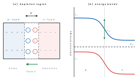
Biasing. Connect a battery across the junction and the barrier changes.
| Forward bias (p to +, n to −) | Reverse bias (p to −, n to +) | |
|---|---|---|
| Applied field | opposes the barrier field | adds to the barrier field |
| Barrier height | reduced to V_B - V | raised to V_B + V |
| Depletion width | narrows | widens |
| Current | large, by majority carriers, mA | tiny, by minority carriers, μA |
| Resistance | low (a few ohms) | very high (megohms) |
A p-n junction conducts freely in one direction and hardly at all in the other. That asymmetry — not any exotic effect — is what makes the junction useful.
Problem. A silicon p-n junction has a barrier potential of 0.70\ \text{V} across a depletion layer 0.50\ \mu\text{m} wide. Find the average electric field in the depletion layer.
What happens to this field when the junction is reverse biased by 5.0\ \text{V}, assuming the width stays the same?
Solution. The average field is the pd divided by the width:
Under 5.0\ \text{V} reverse bias the total pd across the layer is 0.70 + 5.0 = 5.7\ \text{V}, so
an eightfold increase. (In reality W also widens, so the field grows a little less than this.) Fields of this size explain why a junction eventually breaks down.
22.2 Semiconductor diode: Characteristics in forward and reverse bias
A p-n junction with two leads is a junction diode. Its symbol is an arrowhead (the p side, or anode) touching a bar (the n side, or cathode); the arrow points the way conventional current can flow.
To obtain the characteristic, connect the diode in series with a resistor, a milliammeter and a variable pd; record current against voltage; then reverse the battery and repeat with a microammeter.
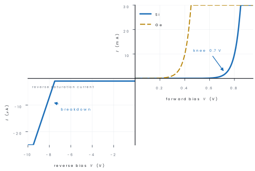
Reading the curve:
- Forward bias. Almost no current until the applied voltage cancels most of the barrier. Beyond this knee (or cut-in) voltage — 0.7\ \text{V} for Si, 0.3\ \text{V} for Ge — the current rises very steeply and is limited only by the external resistance. The curve is non-linear: a diode does not obey Ohm's law.
- Reverse bias. A small, almost constant reverse saturation current of a few microamps, carried by thermally generated minority carriers. It doubles for roughly every 10\ ^\circ\text{C} rise but hardly changes with voltage.
- Breakdown. At a high enough reverse voltage the current suddenly becomes large (avalanche or Zener breakdown). An ordinary diode is destroyed; a Zener diode is designed to work there and is used as a voltage regulator.
The dynamic (a.c.) resistance in the forward region is the reciprocal of the slope at the working point:
The static ratio V/I and the dynamic ratio \Delta V/\Delta I are different numbers for a diode, because the graph is a curve and not a line through the origin. Examiners ask for the dynamic resistance, so always take a small change about the stated point.
Problem.(a) A silicon diode is joined in series with a 1.0\ \text{k}\Omega resistor across a 5.0\ \text{V} supply, connected in forward bias. Taking the diode drop as 0.7\ \text{V}, find the current and the power dissipated in the diode.(b) On the forward characteristic, the current rises from 10\ \text{mA} to 30\ \text{mA} when the voltage goes from 0.70\ \text{V} to 0.74\ \text{V}. Find the dynamic resistance.
Solution.
(a) The resistor carries the whole of the remaining voltage:
(b) r_d = \dfrac{\Delta V}{\Delta I} = \dfrac{0.74-0.70}{(30-10)\times10^{-3}} = \dfrac{0.04}{0.02} = 2\ \Omega.
22.3 Full wave rectification
Rectification is the conversion of alternating current into direct current. A diode does it by conducting only on the half-cycles that forward bias it.
Half-wave rectifier. One diode in series with the load. The negative half of each cycle is simply thrown away, so the output is a series of gaps.
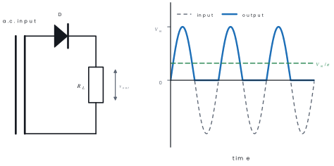
Half-wave rectification wastes half the input. A full-wave rectifier uses both halves; there are two standard circuits.
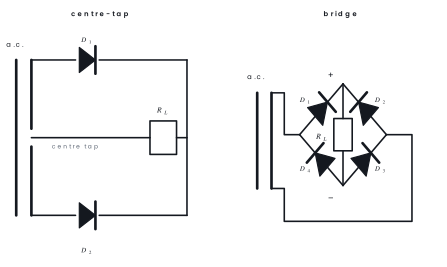
In the centre-tap circuit the transformer secondary is split by an earthed centre tap, so the two halves always have opposite polarity. D_1 conducts while its half is positive, D_2 while the other half is positive; in both cases the current passes downward through R_L.
In the bridge circuit no centre tap is needed: the diagonally opposite pairs D_1D_3 and D_2D_4 conduct alternately, again sending the current one way through the load.
Write the load current on a conducting half-cycle as i = I_m\sin\theta. For a full-wave rectifier the load carries current for the whole cycle, so averaging over half a cycle is enough:
The rectification efficiency is the ratio of d.c. output power to a.c. input power, with r_f the forward resistance of the diode:
For r_f \ll R_L this gives \eta = 8/\pi^{2} = 0.812, i.e. 81.2%. The same working for a half-wave rectifier, averaging over the whole cycle, gives I_{dc}=I_m/\pi, I_{rms}=I_m/2 and \eta = 4/\pi^{2} = 40.6\%.
| Quantity | Half-wave | Full-wave |
|---|---|---|
| I_{dc} | I_m/\pi | 2I_m/\pi |
| V_{dc} | V_m/\pi | 2V_m/\pi |
| I_{rms} | I_m/2 | I_m/\sqrt{2} |
| Max efficiency | 40.6% | 81.2% |
| Ripple factor | 1.21 | 0.48 |
| Output frequency (50 Hz mains) | 50 Hz | 100 Hz |
| PIV per diode | V_m | 2V_m (centre-tap), V_m (bridge) |
The output is still lumpy. A filter — most simply a large capacitor across the load — charges to the peak and discharges slowly between peaks, flattening the ripple.
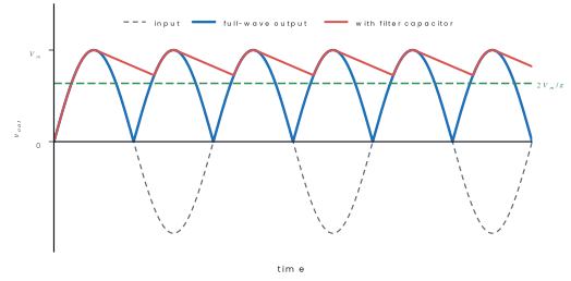
Problem. A centre-tap full-wave rectifier feeds a load of 500\ \Omega. Each half of the transformer secondary gives a peak voltage of 20\ \text{V}. Taking the diodes as ideal, find(a) the peak load current,(b) the d.c. load current and d.c. output voltage,(c) the rms current,(d) the rectification efficiency,(e) the peak inverse voltage across each diode, and (f) the output ripple frequency for a 50 Hz supply.
Solution.
(a) I_m = \dfrac{V_m}{R_L} = \dfrac{20}{500} = 0.040\ \text{A} = 40\ \text{mA}.
(b) I_{dc} = \dfrac{2I_m}{\pi} = \dfrac{2\times40}{3.142} = 25.5\ \text{mA}, and
(c) I_{rms} = \dfrac{I_m}{\sqrt{2}} = \dfrac{40}{1.414} = 28.3\ \text{mA}.
(d) \eta = \dfrac{I_{dc}^{2}}{I_{rms}^{2}} = \left(\dfrac{25.5}{28.3}\right)^{2} = 0.812 = 81.2\% (diodes ideal, so r_f = 0).
(e) When one diode conducts, the other has the whole secondary across it: \text{PIV} = 2V_m = 40\ \text{V}.
(f) Both half-cycles produce an output pulse, so the ripple frequency is 2\times50 = 100\ \text{Hz}.
22.4 Logic gates: NOT, OR, AND, NAND and NOR
A logic gate is a circuit whose input and output voltages are restricted to two levels, written 1 (high, typically +5\ \text{V}) and 0 (low, near 0\ \text{V}). Diodes and transistors make the gates; Boolean algebra describes them.
| Gate | Boolean expression | Read as |
|---|---|---|
| NOT | Y = \bar{A} | inverter |
| OR | Y = A + B | A or B |
| AND | Y = A\cdot B | A and B |
| NAND | Y = \overline{A\cdot B} | AND then NOT |
| NOR | Y = \overline{A+B} | OR then NOT |
The truth tables, which is what the board actually asks you to write:
| A | Y = \bar{A} |
|---|---|
| 0 | 1 |
| 1 | 0 |
| A | B | OR | AND | NAND | NOR |
|---|---|---|---|---|---|
| 0 | 0 | 0 | 0 | 1 | 1 |
| 0 | 1 | 1 | 0 | 1 | 0 |
| 1 | 0 | 1 | 0 | 1 | 0 |
| 1 | 1 | 1 | 1 | 0 | 0 |
The NAND column is the AND column inverted, and NOR is OR inverted — that is all the bar means.
- OR — output 0 only when all inputs are 0.
- AND — output 1 only when all inputs are 1.
- NAND — output 0 only when all inputs are 1.
- NOR — output 1 only when all inputs are 0.
Universal gates. NAND and NOR are called universal because every other gate can be built from copies of just one of them. With NAND:
| Required gate | How to build it from NAND gates |
|---|---|
| NOT | tie both inputs of one NAND together: \overline{A\cdot A} = \bar{A} |
| AND | a NAND followed by a NAND used as NOT |
| OR | invert both inputs with NANDs, then feed a third NAND: \overline{\bar{A}\cdot\bar{B}} = A + B |
The last line is De Morgan's theorem.
Check it for A=B=0, \bar{A}\cdot\bar{B}=1 and the output is 0; for every other combination \bar{A}\cdot\bar{B}=0 and the output is 1 — exactly the OR column.
NAND means AND then NOT. Inverting first and then ANDing gives \bar{A}\cdot\bar{B}, which is NOR, not NAND. Order matters.
22.5 The junction transistor and its configurations
Two junctions back to back in one crystal make a bipolar junction transistor, n-p-n or p-n-p. The emitter is heavily doped and supplies the carriers, the base is very thin and lightly doped, the collector is the largest region.
In normal operation the emitter-base junction is forward biased and the collector-base junction reverse biased, and because the base is thin over 95% of the injected carriers sweep straight through to the collector:
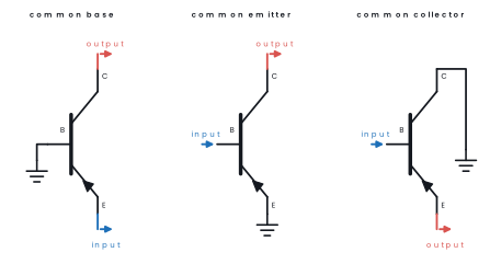
| Configuration | Common terminal | Current gain | Voltage gain | Main use |
|---|---|---|---|---|
| Common base | base | \alpha < 1 | high | high-frequency amplifier |
| Common emitter | emitter | \beta, typically 20–500 | high | general-purpose amplifier, switch |
| Common collector | collector | \approx \beta | < 1 | impedance matching (emitter follower) |
Problem. A transistor has \alpha = 0.98 and an emitter current of 2.0\ \text{mA}. Find the collector current, the base current and the current gain \beta in the common-emitter configuration.
Solution.

Chapter summary
- Diffusion across a p-n junction leaves a depletion region of immobile ions and a barrier potential V_B (0.3 V Ge, 0.7 V Si) that stops further diffusion.
- Forward bias lowers the barrier, narrows the depletion layer and gives a large majority-carrier current; reverse bias does the opposite and leaves only a microamp reverse saturation current until breakdown.
- The diode characteristic is non-linear: no current below the knee voltage, then a steep rise. Dynamic resistance r_d = \Delta V/\Delta I.
- Half-wave: I_{dc}=I_m/\pi, \eta_{max}=40.6\%, ripple 1.21, output 50 Hz.
- Full-wave: I_{dc}=2I_m/\pi, V_{dc}=2V_m/\pi, I_{rms}=I_m/\sqrt{2}, \eta = (8/\pi^{2})R_L/(R_L+r_f), maximum 81.2\%, ripple 0.48, output 100 Hz.
- PIV is V_m for half-wave and bridge, 2V_m for the centre-tap circuit.
- Gates: OR gives 0 only for all-zero inputs; AND gives 1 only for all-one inputs; NAND and NOR are their complements and are universal gates.
- Transistor: I_E = I_B + I_C, \alpha = I_C/I_E, \beta = I_C/I_B = \alpha/(1-\alpha).
Practice questions
Group A — Multiple choice (1 mark each)
- In a p-type semiconductor the majority charge carriers are [1]aelectronsbholescprotonsdpositive ions
- The barrier potential of a silicon p-n junction at room temperature is about [1]a0.1 Vb0.3 Vc0.7 Vd1.4 V
- The maximum efficiency of a full-wave rectifier is [1]a40.6%b50%c81.2%d100%
- The peak inverse voltage across each diode of a centre-tap full-wave rectifier is [1]aV_mb2V_mcV_m/2dV_m/\pi
- A two-input NAND gate gives output 0 only when [1]aboth inputs are 0bboth inputs are 1cany one input is 1dany one input is 0
- For a transistor with \alpha = 0.95, the value of \beta is [1]a9.5b19c95d0.95
Answers to Group A
1. (b) — trivalent dopants create holes.
2. (c) — 0.7 V for Si, 0.3 V for Ge.
3. (c) — \eta_{max} = 8/\pi^{2} = 81.2\%.
4. (b) — the non-conducting diode has the whole secondary across it.
5. (b) — NAND is AND inverted, and AND is 1 only for 1,1.
6. (b) — \beta = \alpha/(1-\alpha) = 0.95/0.05 = 19.
Group B — Short answer (5 marks each)
- Explain how the depletion region and barrier potential are formed at a p-n junction, and state what happens to each under forward and reverse bias. [5]
- Draw the forward and reverse characteristic curves of a junction diode and explain the knee voltage, the reverse saturation current and breakdown. [5]
- A silicon diode in series with a resistor R is connected across a 9.0\ \text{V} battery in forward bias, and the current is 20\ \text{mA}. Find R and the power dissipated in the diode. [5]
- A half-wave rectifier delivers current to a 300\ \Omega load from a supply of peak voltage 30\ \text{V}. Taking the diode as ideal, find the peak current, the d.c. current, the d.c. output voltage and the PIV. [5]
- Draw the truth tables of the NAND and NOR gates, and show how a NAND gate can be used as a NOT gate. [5]
Answers to Group B
3. The diode drops 0.7\ \text{V}, so the resistor has 9.0-0.7 = 8.3\ \text{V} across it and R = 8.3/(20\times10^{-3}) = 415\ \Omega. Power in the diode = 0.7\times20\times10^{-3} = 14\ \text{mW}.
4. I_m = V_m/R_L = 30/300 = 0.10\ \text{A}; I_{dc} = I_m/\pi = 0.10/3.142 = 31.8\ \text{mA}; V_{dc} = I_{dc}R_L = 31.8\times10^{-3}\times300 = 9.55\ \text{V} (which is V_m/\pi); \text{PIV} = V_m = 30\ \text{V}.
5. Outline: write both truth tables from the tables in §22.4. Joining the two inputs of a NAND gives Y = \overline{A\cdot A} = \bar{A}, which is NOT.
Group C — Long answer (8 marks each)
- (a) Draw the circuit of a centre-tap full-wave rectifier and explain its action over one complete cycle, sketching the input and output waveforms. [4](b) Derive expressions for the d.c. current and the rectification efficiency, and hence show that the maximum efficiency is 81.2\%. [4]
- A bridge rectifier is supplied from a transformer whose secondary voltage is 24\ \text{V} rms. The load resistance is 1.0\ \text{k}\Omega and the diodes may be treated as ideal. Find(a) the peak voltage,(b) the peak current,(c) the d.c. output voltage and current,(d) the rms current,(e) the efficiency, and (f) the PIV of each diode. State one advantage of the bridge circuit over the centre-tap circuit. [8]
Answer to Group C question 2
(a) V_m = \sqrt{2}\times24 = 33.9\ \text{V}.
(b) I_m = V_m/R_L = 33.9/1000 = 33.9\ \text{mA}.
(c) V_{dc} = 2V_m/\pi = (2\times33.9)/3.142 = 21.6\ \text{V} and I_{dc} = V_{dc}/R_L = 21.6\ \text{mA}.
(d) I_{rms} = I_m/\sqrt{2} = 33.9/1.414 = 24.0\ \text{mA}.
(e) \eta = (I_{dc}/I_{rms})^{2} = (21.6/24.0)^{2} = 0.81 = 81\%.
(f) For a bridge, \text{PIV} = V_m = 33.9\ \text{V}.
Advantage: no centre-tapped transformer is needed, and the PIV per diode is only V_m instead of 2V_m, so cheaper diodes can be used for the same output.
Group D — Model answers for long questions (10 marks each, for deeper revision)
- Explain, with a circuit diagram description, the working of a full-wave bridge rectifier, and calculate its output with and without a filter. [10]
- Explain the working of an n-p-n transistor as a common-emitter amplifier and define its current gains. [10]
Model answer D1: the full-wave bridge rectifier (10 marks)
Introduction. A rectifier converts alternating current into direct current. A p–n junction diode conducts only when it is forward biased, so it can be used for this purpose. A full-wave rectifier uses both half-cycles of the input.
Circuit. Four diodes D_{1}–D_{4} form a bridge. The a.c. supply (from the secondary of a transformer) is joined to two opposite corners of the bridge, and the load resistor R_{L} is connected across the other two corners.
Working.
- Positive half-cycle. The upper input terminal is positive. Diodes D_{1} and D_{3} are forward biased and conduct, while D_{2} and D_{4} are reverse biased. The current flows through the load from top to bottom.
- Negative half-cycle. The polarity reverses. Now D_{2} and D_{4} conduct and D_{1} and D_{3} are off, but the current again passes through R_{L} in the same direction.
- The output voltage is therefore a series of positive humps, one for every half-cycle of the input, and its frequency is twice the input frequency: 100 Hz for a 50 Hz supply.
Output of the bridge. If V_{p} is the peak input voltage and each conducting diode drops 0.7\ \text{V} (two diodes are in series), the peak output is V_{p} - 1.4\ \text{V}.
The average (d.c.) value is V_{dc} = 2V_{peak}/\pi = 0.636\,V_{peak}, and the rms value is V_{peak}/\sqrt{2}.
The ripple factor of a full-wave rectifier without a filter is 0.48, compared with 1.21 for a half-wave rectifier, and its theoretical efficiency is 81.2%, double that of the half-wave circuit (40.6%).
Filter. A capacitor connected across the load charges to the peak voltage and discharges slowly through R_{L} between the peaks, which smooths the ripple. A larger capacitance or a larger R_{L} gives a flatter output.
| Feature | Half-wave | Full-wave bridge |
|---|---|---|
| Diodes | 1 | 4 |
| Output frequency | f | 2f |
| V_{dc} | V_{peak}/\pi | 2V_{peak}/\pi |
| Ripple factor | 1.21 | 0.48 |
| Efficiency | 40.6% | 81.2% |
| Transformer centre tap | Not needed | Not needed in a bridge |
Numerical. A transformer gives 12\ \text{V} rms. The peak is 12\sqrt{2} = 16.97\ \text{V}, the peak output after the two diode drops is 16.97 - 1.4 = 15.57\ \text{V}, and the average d.c. output is 2(15.57)/\pi = 9.91\ \text{V}.
A capacitor raises the d.c. output almost to 15.6\ \text{V}.
Conclusion. The bridge rectifier uses both half-cycles with four diodes, and it is the circuit inside a mobile phone charger.
Model answer D2: the transistor as a common-emitter amplifier (10 marks)
Introduction. A junction transistor has three regions, the emitter (heavily doped), the thin base and the collector. An n-p-n transistor has a thin p-type base between two n-type regions.
In an amplifier the emitter–base junction is forward biased and the collector–base junction is reverse biased.
Current relations. I_{E} = I_{B} + I_{C}. The base current is only about 1–5% of the emitter current, because the base is very thin and lightly doped.
Current gains.
- Common-base current gain \alpha = I_{C}/I_{E} (slightly less than 1, typically 0.95–0.99).
- Common-emitter current gain \beta = I_{C}/I_{B} (typically 20–200).
- The two are related by \beta = \dfrac{\alpha}{1 - \alpha}.
Working as an amplifier. The signal is applied between the base and the emitter, and the output is taken from the load resistor R_{C} in the collector circuit.
- A small change \Delta I_{B} in the base current produces a large change \Delta I_{C} = \beta\,\Delta I_{B} in the collector current.
- The voltage drop across R_{C} changes by \Delta I_{C} R_{C}, so the small input voltage is converted into a much larger output voltage.
- In the positive half-cycle of the input the collector current rises, so V_{CE} = V_{CC} - I_{C}R_{C} falls. The output is therefore 180° out of phase with the input.
Gain. Voltage gain A_{v} = \dfrac{\Delta V_{out}}{\Delta V_{in}} = \beta\,\dfrac{R_{C}}{R_{in}}, where R_{in} is the input resistance. The power gain is \beta \times A_{v}.
| Configuration | Input terminals | Output terminals | Phase | Use |
|---|---|---|---|---|
| Common emitter | Base–emitter | Collector–emitter | 180° | General amplifier, switch |
| Common base | Emitter–base | Collector–base | 0° | High-frequency |
| Common collector | Base–collector | Emitter–collector | 0° | Buffer, impedance matching |
Numerical. When I_{B} is 40\ \mu\text{A} and I_{C} is 2.0\ \text{mA}, \beta = 2.0\times10^{-3}/40\times10^{-6} = 50 and I_{E} = 2.04\ \text{mA}, so \alpha = 2.0/2.04 = 0.98 and the check \beta = 0.98/0.02 = 49 agrees within rounding.
With R_{C} = 4\ \text{k}\Omega and R_{in} = 1\ \text{k}\Omega the voltage gain is 50 \times 4000/1000 = 200.
Conclusion. The common-emitter circuit gives both current and voltage gain, which makes it the most widely used amplifier.
Practise more: Physics question bank